Page 11 of 76
Re: It didn't explode....... YET (aka niges amp)
Posted: Tue Aug 23, 2016 3:09 pm
by nige2000
Aghh.... I Don't get it
Theres no gnd pin on the lm3875 and other pins are not connected to gnd other than through caps or resistors
The only way +33 can get returned to gnd is through v- and the first 10 cells meaning the only noise contamination on the pcb would be from filter caps if installed?
Re: It didn't explode....... YET (aka niges amp)
Posted: Tue Aug 23, 2016 3:46 pm
by jkeny
nige2000 wrote:Aghh.... I Don't get it
Theres no gnd pin on the lm3875 and other pins are not connected to gnd other than through caps or resistors
The only way +33 can get returned to gnd is through v- and the first 10 cells meaning the only noise contamination on the pcb would be from filter caps if installed?
It's the same in all dual supply opamps - there's an internal ground through the negative(inverting) or positive(non-inverting) input pins (pin 8 or 7)
In your & Peter's config the input is through pin 7 (positive input) & pin 8 (neg input) is connected to ground via R3.
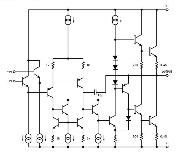
If you look at the internal schematic of LM3875 in the datasheet, you will see that it is differential input/single-ended output but you are using it as single ended input, so one input is tied to ground.
If the V+ return currents were going back through V- then a bypass cap across V+ & V- would be needed, not across V+ & GND
Have a look here at the diagram & text
http://phonoclone.com/diy-gc.html
Grounding is critical. The output signal must not share any of the inverting input ground path. I recommend a binary star ground as follows: Two ground points are defined, the base of R2 is the signal ground S and the base of R3 the power ground P. Attach all the S grounds together, and all the P grounds together, and then connect the two grounds by a single wire. (Note: The RCA input ground can go to the base of the attenuator, rather than R2.) The case can be left floating or attached to the signal ground. The chips should be well heatsinked, but electrically isolated from the heatsink. An isolated version of the LM3875 exists (LM3875TF) which makes this easy to do.
The text in italics is what I was suggesting
Re: It didn't explode....... YET (aka niges amp)
Posted: Tue Aug 23, 2016 11:40 pm
by nige2000
jkeny wrote:nige2000 wrote:Aghh.... I Don't get it
Theres no gnd pin on the lm3875 and other pins are not connected to gnd other than through caps or resistors
The only way +33 can get returned to gnd is through v- and the first 10 cells meaning the only noise contamination on the pcb would be from filter caps if installed?
It's the same in all dual supply opamps - there's an internal ground through the negative(inverting) or positive(non-inverting) input pins (pin 8 or 7)
In your & Peter's config the input is through pin 7 (positive input) & pin 8 (neg input) is connected to ground via R3.
all power been returned though a 680r resistor r3?
If you look at the internal schematic of LM3875 in the datasheet, you will see that it is differential input/single-ended output but you are using it as single ended input, so one input is tied to ground.
through 680r surely thats just for input signal return?
If the V+ return currents were going back through V- then a bypass cap across V+ & V- would be needed, not across V+ & GND
Have a look here at the diagram & text
http://phonoclone.com/diy-gc.html
Grounding is critical. The output signal must not share any of the inverting input ground path. I recommend a binary star ground as follows: Two ground points are defined, the base of R2 is the signal ground S and the base of R3 the power ground P. Attach all the S grounds together, and all the P grounds together, and then connect the two grounds by a single wire. (Note: The RCA input ground can go to the base of the attenuator, rather than R2.) The case can be left floating or attached to the signal ground. The chips should be well heatsinked, but electrically isolated from the heatsink. An isolated version of the LM3875 exists (LM3875TF) which makes this easy to do.
The text in italics is what I was suggesting
when he says power gnd is that not just a figure of speech for lesser priority non signal gnds
Re: It didn't explode....... YET (aka niges amp)
Posted: Wed Aug 24, 2016 12:34 am
by jkeny
nige2000 wrote:all power been returned though a 680r resistor r3?
What I'm saying is that one leg of the input is tied to ground & this is therefore the ground reference to which output & power needs to be tied.
As I said , If the V+ return currents were going back through V- then a bypass cap across V+ & V- would be needed, not across V+ & GND
Have a look here at the diagram & text
http://phonoclone.com/diy-gc.html
Grounding is critical. The output signal must not share any of the inverting input ground path. I recommend a binary star ground as follows: Two ground points are defined, the base of R2 is the signal ground S and the base of R3 the power ground P. Attach all the S grounds together, and all the P grounds together, and then connect the two grounds by a single wire. (Note: The RCA input ground can go to the base of the attenuator, rather than R2.) The case can be left floating or attached to the signal ground. The chips should be well heatsinked, but electrically isolated from the heatsink. An isolated version of the LM3875 exists (LM3875TF) which makes this easy to do.
The text in italics is what I was suggesting
when he says power gnd is that not just a figure of speech for lesser priority non signal gnds
The base of R3 in his diagram is power ground but I think what you are saying is that without the bypass caps there would be no power ground, just signal & output grounds, right?

But can I ask, what are you connecting the midpoint of your battery pack to? Whatever you are connecting this to is your power ground point - it's where the supply currents return to, both positive & negative supplies
Re: It didn't explode....... YET (aka niges amp)
Posted: Wed Aug 24, 2016 10:25 am
by nige2000
jkeny wrote:
The base of R3 in his diagram is power ground but I think what you are saying is that without the bypass caps there would be no power ground, just signal & output grounds, right?
yea thats the way im looking at it
But can I ask, what are you connecting the midpoint of your battery pack to? Whatever you are connecting this to is your power ground point - it's where the supply currents return to, both positive & negative supplies
midpoint of battery pack is connected to signal gnd in and out and speaker return
but if the op amp has no ground pin and v in- (in this case) is used as return for signal input and not a return for v+ and v-
v+ must be returning through v- through 10 lifepo4 cells to get to battery pack gnd by then should be very well filtered?
Re: It didn't explode....... YET (aka niges amp)
Posted: Wed Aug 24, 2016 11:13 am
by nige2000
i see an explanation on the one cap or two on dual op amps here
http://electronics.stackexchange.com/qu ... tor-or-two
If the output load is primarily to ground, then two capacitors. If it's to either supply, then one capacitor will suffice.
The purpose of bypass capacitors is to provide a low-impedance close to the chip (bypassing any series inductance to the supply rails). Since most op-amps do not have a ground pin the internal circuitry does not care about the ground level, however when you apply a load to ground the current path is from the positive or negative supply, through the circuitry on the chip, out the output and through the load to ground. A capacitor from the positive and negative supplies will make sure that loop is physically small and thus low inductance.
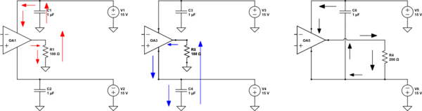
The left two schematics show an op-amp driving positive and negative current into a load connected to ground, and how the bypass capacitor appears in the loop. The right hand one shows a load connected to the negative rail. The capacitor in the right hand schematic is twice as effective with the load connected this way (1uF rather than 500nF) and it saves a part.
Re: It didn't explode....... YET (aka niges amp)
Posted: Wed Aug 24, 2016 11:51 am
by frd1996
John,
I had a thought about your comments about PCB layout. Essentially we are talking about one of the two configurations shown below.
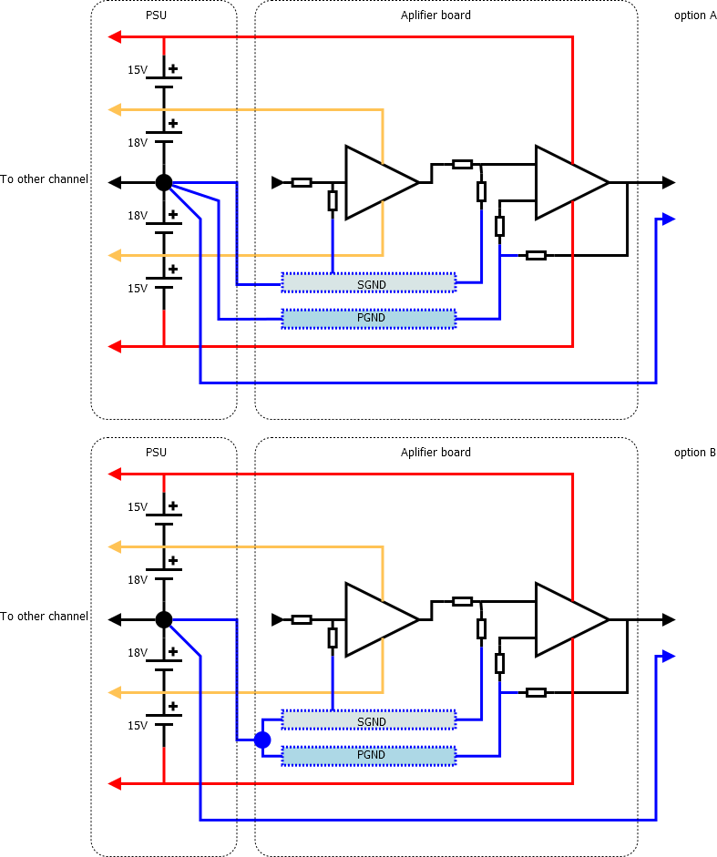
- nige_topology1.png (34.77 KiB) Viewed 419 times
I also believe that this is the PSU arrangement that Nige is planning to use. Where would you connect the "bottoms" of decoupling caps (not shown on the diagram): PGND, SGND, the central GND point between he bateries, somewhere else?
F
Re: It didn't explode....... YET (aka niges amp)
Posted: Wed Aug 24, 2016 1:26 pm
by jkeny
nige2000 wrote:i see an explanation on the one cap or two on dual op amps here
http://electronics.stackexchange.com/qu ... tor-or-two
If the output load is primarily to ground, then two capacitors. If it's to either supply, then one capacitor will suffice.
The purpose of bypass capacitors is to provide a low-impedance close to the chip (bypassing any series inductance to the supply rails). Since most op-amps do not have a ground pin the internal circuitry does not care about the ground level, however when you apply a load to ground the current path is from the positive or negative supply, through the circuitry on the chip, out the output and through the load to ground. A capacitor from the positive and negative supplies will make sure that loop is physically small and thus low inductance.
The left two schematics show an op-amp driving positive and negative current into a load connected to ground, and how the bypass capacitor appears in the loop. The right hand one shows a load connected to the negative rail. The capacitor in the right hand schematic is twice as effective with the load connected this way (1uF rather than 500nF) and it saves a part.
Right & your output is primarily to ground i.e it swings positive going & negative going around ground driving a loudspeaker.
If you were only interested in positive going outputs you would leave out the battery mid-point as your ground & use the negative pole of your battery bank as the ground point. The reverse if you were only interested in negative going output.
I know you want to track the PS currents through the opamps internal circuitry to understand the current flow but I think an opamp is a type of differential circuit which only compares the differences between the two inputs, applies a gain to this difference & outputs this increased voltage or current through its output. This is a single ended output but if it was a balanced output then we would not need to reference anything to ground - we could run the + & - outputs directly to the speakers & everything would work fine
You may be right, Nige that capacitors only slow down the current delivery in battery operation but in designing a pcb, I would consider it wise to include pads for them.
Re: It didn't explode....... YET (aka niges amp)
Posted: Wed Aug 24, 2016 1:46 pm
by jkeny
frd1996 wrote:John,
I had a thought about your comments about PCB layout. Essentially we are talking about one of the two configurations shown below.
nige_topology1.png
I also believe that this is the PSU arrangement that Nige is planning to use. Where would you connect the "bottoms" of decoupling caps (not shown on the diagram): PGND, SGND, the central GND point between he bateries, somewhere else?
F
Conceptually, I would go with option A - option B might introduce a small ground current potential difference between channels
Decoupling caps should be located as close to the LM3875's +/- supply pins as possible. You want the smallest loop possible for the currents to circulate.
The idea of decoupling caps is to provide a low impedance supply for the instantaneous current demands of the LM3875. I have determined from experience that these batteries have superbly low internal impedance (single milliohm region) which satisfies this & we also determined that capacitors which I've tried seemed to slow down this speed of current delivery. I haven't done much experimenting with power amplifiers, Nige is doing this & he seems to come to the same conclusion with power amplifiers. So it may be that batteries without bypass caps are the best solution - the impedance of the wires & pcb tracks between battery supply & the LM3875 could limit the speed of current delivery but Nige reports that this amp's speed is one of it's defining characteristics consideration so it would appear not to be an issue. The other consideration if using capacitors is to use ones which have low esr or impedance, otherwise these will slow down current delivery when compared to battery.
Re: It didn't explode....... YET (aka niges amp)
Posted: Wed Aug 24, 2016 1:55 pm
by nige2000
jkeny wrote:
You may be right, Nige that capacitors only slow down the current delivery in battery operation but in designing a pcb, I would consider it wise to include pads for them.
sure is easier to have the pads and not use them than the other way round
i used these for bypass on the prototype
http://ie.farnell.com/wima/smdtc04220tb ... dp/1890111
id be inclined to test something along these lines
these film type caps dont seem to have the same slowing effect that alot of caps have with the batteries